MooreElite Assembly Services, relying on the long-term strategic cooperation with TOP OSAT, provides one-stop assembly sevevice . Provided guarantee for the delivery, capacity and quality.

MooreElite Assembly Services, relying on the long-term strategic cooperation with TOP OSAT, provides one-stop assembly sevevice . Provided guarantee for the delivery, capacity and quality.
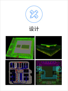
Substrate/Framework Design
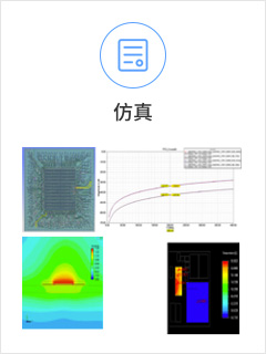
Chip/Package/Substrate Co-Simulation:Including Package structure stress, Signal Integrity, Power Integrity, thermal optimization
Wafer Level Package, Fanout Design, Ceramic, Metal Packaging Design
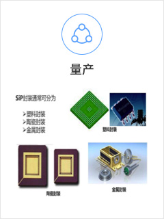
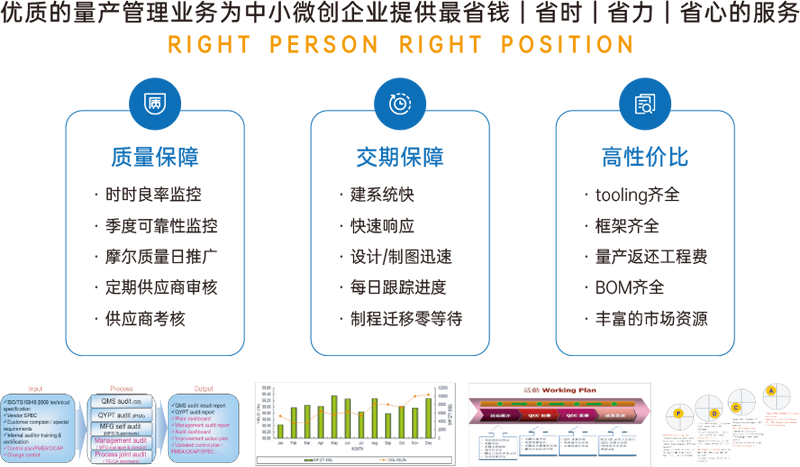
Package Mass Production Management
Link customer directly to OSAT
Business status: mass production customers have reached 53, with shipments reaching 63.5KK/ month.
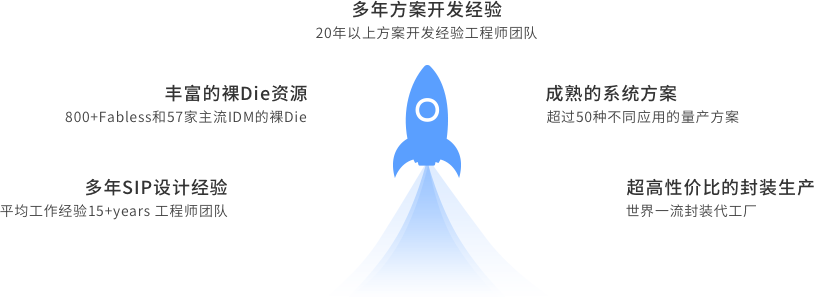
MooreElite provides SiP services from solution development, substrate design, simulation, proofing and mass production. Moore elite has rich naked die resources, more than 25 years of experience in the solution development engineering team, 17 years of experience in the SiP design team, more than 50 SiP mass production solutions, the world's top three packaging resources. It has become a qualified supplier of CRRC, a partner of Bosch, a driverless partner of didi and a partner of top domestic universities and research institutes.


- Die positioning variation less than 20um variation.
- The best wire bonding quality with advanced soldering technology.
- SiP package above 99.7% yield for production.
- Great customer satisfaction with small size, excellent performance, and proprietary security.
Application:Photoelectric Sensor Module;
Internal devices(14):Logic Gate Chip + Regulator + Triode + Diode+ Resistance Capacitance;
Advantage:Small size, low cost, strong confidentiality, easy installation.
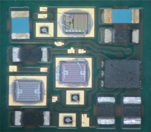
Application:Vehicle Sensing System;
Internal devices (19):MCU + Millimeter Wave Chip + Humidity Sensor Chip + Optical Sensor Chip + Resistance Capacitor + Battery;
Advantage:High Integration, Transparent Packaging, MEMS Packaging.

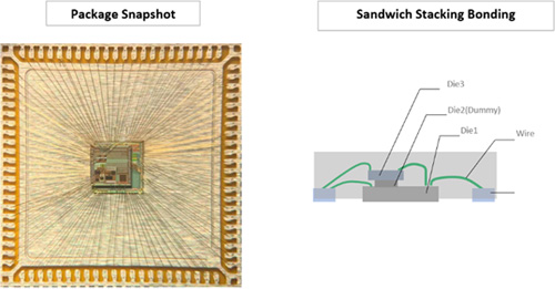
Device information 1:
Package type:QFN88L
Package size:10X10X0.75mm
Die size:2.2X2.1mm/2.3x2.2mm
Wire dimeter:0.8mil Au wire
Bond pad opening:52x54um
Bond pad pitch:70um
Technical challenges:With the “sandwich” lamination process, the problems such as wire sag and chip hidden crack are easy to occur due to three-time chip attaching and two-time wire bonding process. Because the top chip of the product is larger than the second layer chip (fake chip) which makes the lower part of the wire bonding area belongs to the suspended position. It will cause the phenomenon of poor welding by the shaking of the top chip during the wire bonding process. Therefore, high-precision chip attachment machine is adopted to control the chip placement error within 20um, and the most advanced multi-stage welding process is adopted in the wire bonding process to avoid poor welding problems. All these make the packaging yield over 99.7%, and no problems are found in the customer function test.

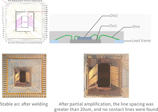
Device information 2:
Package type:QFN68L
Package size:8X8X0.75mm
Die size:2.2X2.1mm/2.3x2.2mm
Wire dimeter:0.7mil Au wire
Bond pad opening:45x48um
Bond pad pitch:54um
Technical challenges:With the two-layer chip lamination process, the angle of the wire from die1 to die2 is very inclined, the included angle is more than 45 degrees and the wire gap is less than twice wire diameter, which has exceeded the packaging design specification; on the other hand, because of the BPO (bond pad Opening) limit only 0.7mil gold wire can be used which will cause instable wire loop lead to wire touching problem during wire bonding process. Therefore, the most advanced PSL multi-stage ultra-low wire loop is adopted to realize the stability wire loop by controlling the bending point, height and tightness of wire loop. All these make the packaging yield over 99.5%, and no problems are found in customer test.

留下您的需求,我们会第一时间与您联系
留下您的任意需求
我们都会第一时间和您联系


